


 Call
Call SEMICONDUCTOR ICs RELIABILITY
Automotive, Defence, Aerospace

Industrial, IoT, Communication

ELECTRONIC MODULES RELIABILITY
ECU for Automotive

ECU for Aerospace & Defence

Smart digital solutions for your productivity close to you
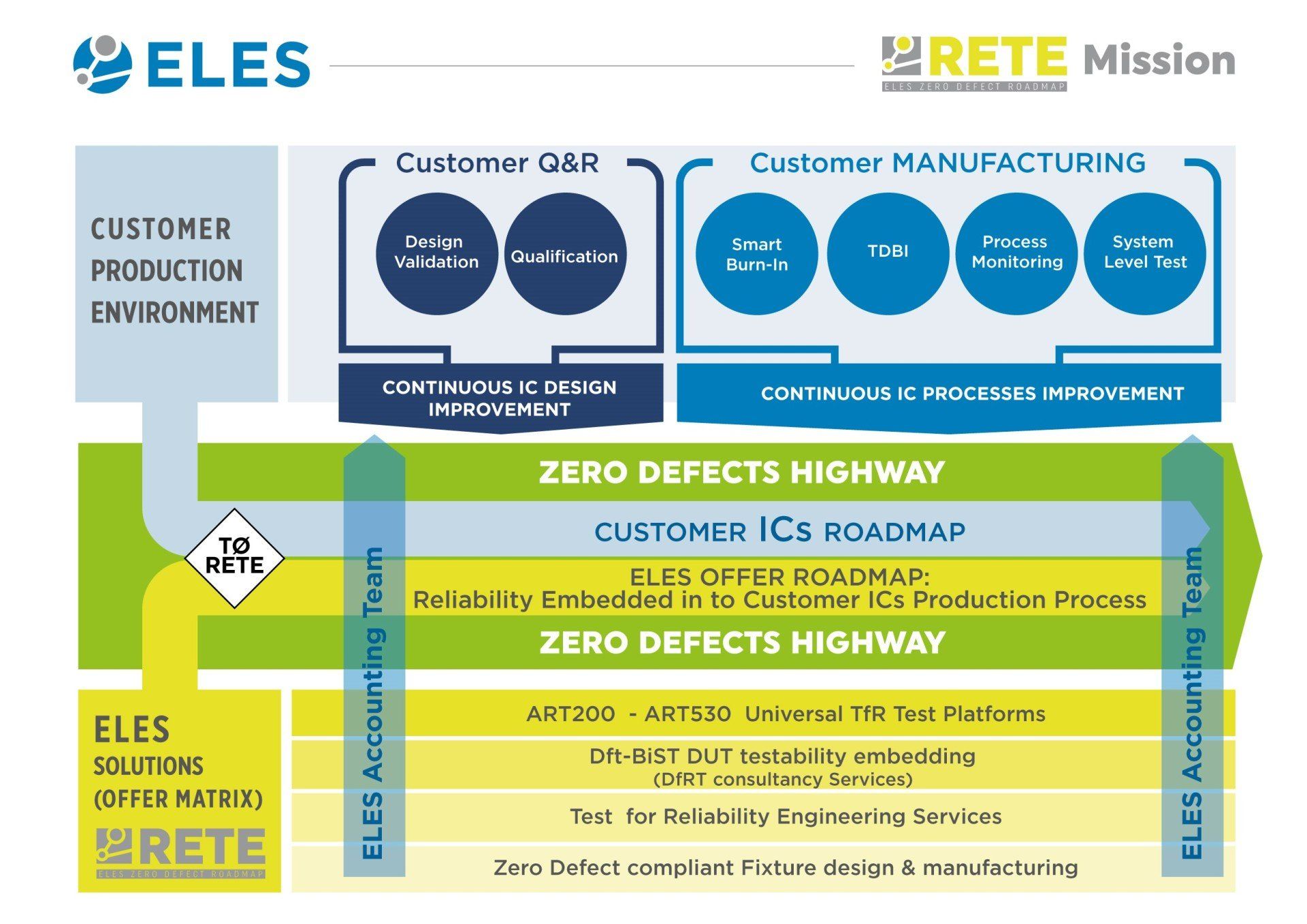
ELES has developed specific solutions for Design, Qualification and Manufacturing of MEMORIES, Full Digital or Mixed Signal SOC (Systems On Chip), ADAS (Advanced Driver-Assistance Systems), u-EMBEDDED MEMORY, SMART POWER, SMART LEDS and MEMS (Micro Electrical-Mechanical Systems). Thanks to RETE approach and the possibility of achieving the target of Zero Defects, ELES solutions and services are mostly used in markets such as automotive, avionics, aerospace and defence, where semiconductors reliability is fundamental for safety.However, the innovation brought by ELES with RETE is also applied in more price sensitive sectors such as industrial, communications and IOT where design and process improvement generated by RETE allow sensible cost reductions.A major source of errors in modern integrated circuits are intermittent faults. The root cause for these faults ranges from manufacturing residuals to oxide breakdown. Intermittent faults may or may not always induce an error depending on some environmental conditions, but when it does, it occurs in the same location due to unstable or marginal hardware. Their occurrence is expected to increase because of the higher circuit complexity and the aggressive scaling of semiconductor devices. In the traditional reliability flow, defective devices are identified doing parametric and functional measurements on ATE machines before and after having stressed the device. Failures which are intermittent are not identified, as they tend to remain activated so long as the stress conditions are present.
RETE business model
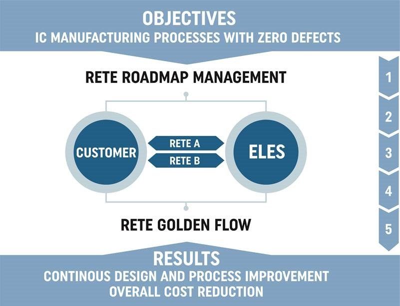
In order to detect early and intermittent failures and move towards a zero defect semiconductors production process, ELES has developed the innovative reliability test approach called RETE (Reliability Embedded Test Engineering). Reliability tests are embedded into all Design, Qualification and Manufacturing IC production as follows:
ELES TEST PLATFORMS
The test platform generates the stimuli to be applied to the Devices Under Test (DUTs), which can be selected individually and measures their responses. ELES test platforms are universal.
The modular design, the use of re-programmable FPGA-based hardware, the possibility to add expansion modules and a wide range of available test libraries, allow the use of the same platform as:
• Development Station
• Qualification & Reliability Testbench
• Massively Parallel Test during Burn In equipment
and can be used for:
• for reliability tests of MEMORIES, MEMS (Micro Electrical-Mechanical-Systems)
• Full Digital or Mixed Signal SOC (Systems On Chip)
• ADAS (Advanced Driver-Assistance Systems)
• u-EMBEDDED MEMORY, SMART POWER
• SMART LEDs according to AEC Q100 / JEDEC JESD-22-A10x.
A Processing Unit integrated into the test driver analyzes real time the test results, adapting the sequence and the time of test according to the device status.
It runs complex characterization functions and generates detailed information about the measured values. In the case of device failure, is able to run further measurements and implement device recovery algorithms.
Every test platform is connected, via a suitable interface, with one board containing the devices to be tested.
ELES Universal Platforms are ART200 and the ART2020.
TEST SYSTEM CONFIGURATIONS
In order to detect early and intermittent failures and move towards a zero defect semiconductors production process, ELES has developed the innovative reliability test approach called RETE (Reliability Embedded Test Engineering).
Reliability tests are embedded in to all Design, Qualification and Manufacturing IC production as follows:
ELES SERVICES
- Design for Reliability Test (DfRT) Consultancy: Consulting activity for the designer carried out in the concept phase of the device and aimed at optimizing the testability and observability of the device blocks and functions to improve the devices quality and reliability.
- Test for Reliability (TfR) Consultancy: Consultancy activity carried on during the definition of the reliability test, oriented to the definition of the key parameters to be monitored, of the data to be collected, of the flow to be implemented.
- Application Development Support (ADS): Analysis of customer’s device specifications and trial requirements which allow ELES to design fit for purpose Fixtures, Test programs for the specific applications. During this phase ELES will partner with the customers Device designers, Q&R and Test engineers.
- SIGNAL INTEGRITY post layout Simulation: Signal Integrity Post Layout Simulation based on ART tester + Interface board + Fixture + DUT Model simulation (IBIS or SPICE models). Data Analysis, Circuit and Layout Parameters Tuning to achieve optimal SI performances of the Application on the specific DUT.
- Power INTEGRITY post layout Simulation: Power Integrity Post layout simulation based on ART Tester + Interface board + Fixture layouts to evaluate the quality of power supply levels and possible fine tuning of the fixture layout.
- Test for Reliability (TfR) configuration: Definition for each single test of the sequence of stress and tests and data logging
- Test Program Development: Test Program code development according to Device Test list Specification and Test for Reliability flow
- Test Pattern Generation: Generation of the stimuli - in Eles proprietary format - starting from Device Datasheet and/or Test Pattern Specification
- Device Diagnostic Descr & Decode: Device diagnostic registers interpretation and analog measurement description for the use of Real Time SW Interpreter
- Application Integration: Verification of the first board on test bench based on the trial specification. Followed by its integration with the DUT and test program, and the validation of the whole package at ambient temperature. An application report is then generated and shared with the client for approval.
- DUT Functional characterization: Characterization of the devices ambient functional behavior based upon agreed electrical and functional parameters not including temperature. The results of the test will be inserted in to the Application Integration report
- DUT Thermal characterization: Characterization of the devices thermic behavior in a temp range with the objective of defining the trial setup. The results of the test will be inserted in to the Application Integration report
- Data Analysis For Reliability Improvement: Analysis of the data collected during the trial execution with the aim of finding Root Causes of the defects.
- Socket Functional Verification: ELES will verify the chosen socket and device package to ensure the functional integration against final application. This excludes verification of the socket against the data sheet. The results of the test will be inserted in to the Application Integration report.


